- 您现在的位置:买卖IC网 > Sheet目录337 > LE25S40MB-AH (ON Semiconductor)IC MEM 4MBIT SERIAL FLASH 8SOP
�� �
�
�LE25S40MB�
�Device� Operation�
�The� read,� erase,� program� and� other� required� functions� of� the� device� are� executed� through� the� command� registers.� The�
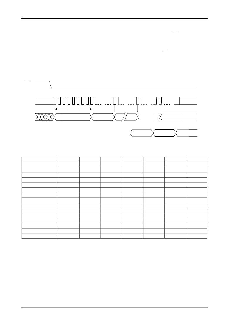
�serial� I/O� corrugate� is� shown� in� Figure� 3� and� the� command� list� is� shown� in� Table� 2.� At� the� falling� CS� edge� the� device� is�
�selected,� and� serial� input� is� enabled� for� the� commands,� addresses,� etc.� These� inputs� are� normalized� in� 8� bit� units� and�
�taken� into� the� device� interior� in� synchronization� with� the� rising� edge� of� SCK,� which� causes� the� device� to� execute�
�operation� according� to� the� command� that� is� input.�
�The� LE25S40MB� supports� both� serial� interface� SPI� mode� 0� and� SPI� mode� 3.� At� the� falling� CS� edge,� SPI� mode� 0� is�
�automatically� selected� if� the� logic� level� of� SCK� is� low,� and� SPI� mode� 3� is� automatically� selected� if� the� logic� level� of�
�SCK� is� high.�
�Figure� 3� I/O� waveforms�
�CS�
�Mode3�
�SCK�
�Mode0�
�8CLK�
�SI�
�MSB�
�(Bit7)�
�1st� bus�
�LSB�
�(Bit0)�
�2nd� bus�
�Nth� bus�
�SO�
�High� Impedance�
�DATA�
�DATA�
�Table� 2� Command� Settings�
�Read�
�Command�
�1st� bus� cycle�
�03h�
�0Bh�
�2nd� bus� cycle�
�A23-A16�
�A23-A16�
�3rd� bus� cycle�
�A15-A8�
�A15-A8�
�4th� bus� cycle�
�A7-A0�
�A7-A0�
�5th� bus� cycle�
�RD� *1�
�X�
�6th� bus� cycle�
�RD� *1�
�RD� *1�
�Nth� bus� cycle�
�RD� *1�
�RD� *1�
�Small� sector� erase�
�Sector� erase�
�20h� /� D7h�
�D8h�
�A23-A16�
�A23-A16�
�A15-A8�
�A15-A8�
�A7-A0�
�A7-A0�
�Chip� erase�
�60h� /� C7h�
�Page� program�
�02h�
�A23-A16�
�A15-A8�
�A7-A0�
�PD� *2�
�PD� *2�
�PD� *2�
�Write� enable�
�Write� disable�
�Power� down�
�Status� register� read�
�06h�
�04h�
�B9h�
�05h�
�Status� register� write�
�JEDEC� ID� read�
�01h�
�9Fh�
�DATA�
�ID� read�
�ABh�
�X�
�X�
�X�
�power� down�
�Exit� power� down� mode�
�B9h�
�ABh�
�Explanatory� notes� for� Table� 2�
�"X"� signifies� "don't� care"� (that� is� to� say,� any� value� may� be� input).�
�The� "h"� following� each� code� indicates� that� the� number� given� is� in� hexadecimal� notation.�
�Addresses� A23� to� A19� for� all� commands� are� "Don't� care".�
�*1:� "RD"� stands� for� read� data.� *2:� "PD"� stands� for� page� program� data.�
�No.A2096-4/22�
�发布紧急采购,3分钟左右您将得到回复。
相关PDF资料
LE25U20AMB-AH
IC MEM 2MBIT SERIAL FLASH 8SOP
LFDAS12XSIT
HARDWARE MC9S12XS 112-PIN
LFXP10E-L-EV
BOARD EVAL LATTICEXP10E STD
LH28F008SCHT-TE
IC FLASH 8MBIT 85NS 40TSOP
LH28F160S3HNS-TV
IC FLASH 16MBIT 100NS 56SSOP
LH28F160S5HNS-S1
IC FLASH 16MBIT 70NS 56SSOP
LH28F320S3HNS-ZM
IC FLASH 32MBIT 110NS 56SSOP
LH28F320SKTD-ZR
IC FLASH 32MBIT 70NS 48TSOP
相关代理商/技术参数
LE25S40QES00-AH
制造商:ON Semiconductor 功能描述:S-FLASH MEMORY(4M) - Tape and Reel
LE25S67EKS-GD0000
制造商:Legacy Electronics Inc 功能描述:512MB PC2-5300 CL5 DIMM - Bulk
LE25S80MB-AH
制造商:ON Semiconductor 功能描述:8M BIT SERIAL FLASH MEMOR - Tape and Reel 制造商:ON Semiconductor 功能描述:Flash 制造商:ON Semiconductor 功能描述:REEL - 8M BIT SERIAL FLASH MEMOR
LE25S81MCTWG
制造商:ON Semiconductor 功能描述:8M BIT SERIAL FLASH MEMOR - Tape and Reel 制造商:ON Semiconductor 功能描述:REEL - 8M BIT SERIAL FLASH MEMOR
LE25SS53DKE-CAR
制造商:Legacy Electronics Inc 功能描述:512MB PC2-4200 (533 MHZ) CL4-4-4,200 PIN SODIMM GOLD 1.181" - Bulk
LE25U20AMB
制造商:SANYO 制造商全称:Sanyo Semicon Device 功能描述:2M-bit (256K??8) Serial Flash Memory
LE25U20AMB-AH
功能描述:闪存 S-FLASH MEMORY(2M)
RoHS:否 制造商:ON Semiconductor 数据总线宽度:1 bit 存储类型:Flash 存储容量:2 MB 结构:256 K x 8 定时类型: 接口类型:SPI 访问时间: 电源电压-最大:3.6 V 电源电压-最小:2.3 V 最大工作电流:15 mA 工作温度:- 40 C to + 85 C 安装风格:SMD/SMT 封装 / 箱体: 封装:Reel
LE25U20AMBM02-AH
功能描述:闪存 RoHS:否 制造商:ON Semiconductor 数据总线宽度:1 bit 存储类型:Flash 存储容量:2 MB 结构:256 K x 8 定时类型: 接口类型:SPI 访问时间: 电源电压-最大:3.6 V 电源电压-最小:2.3 V 最大工作电流:15 mA 工作温度:- 40 C to + 85 C 安装风格:SMD/SMT 封装 / 箱体: 封装:Reel